PCB TOOLS / PINOUT & INTERFACE REFERENCE
Arduino Uno R3 Pinout, Ports and ICSP Reference
Compare Uno R3 power, digital, analog, SPI/I²C/UART pins and both ICSP headers. Board D/A labels are distinguished from ATmega328P package pin numbers.
Quick answer
Uno R3 is based on ATmega328P. D0/D1 are RX/TX; D10–D13 are SS/MOSI/MISO/SCK; A4/A5 are SDA/SCL. The extra R3 SDA/SCL header duplicates A4/A5 and is not a second independent I²C bus.
Scope
Applies to classic Uno R3/ATmega328P. Parenthesized MCU pin numbers follow the source 28-pin DIP package, not an SMD package. Uno R4 uses Renesas RA4M1 and does not inherit these AVR ports, timers or package numbers. The original diagram groups functions; it is not a board photo or dimensioned mechanical layout.
Reading example
For main-MCU SPI, use D11=MOSI, D12=MISO and D13=SCK, or the same signals on the main 2×3 ICSP header; D10 is commonly chip select. The other ICSP header near the USB interface programs the ATmega16U2, not the main MCU.
Interfaces, pinouts and technical reference
Arduino Uno
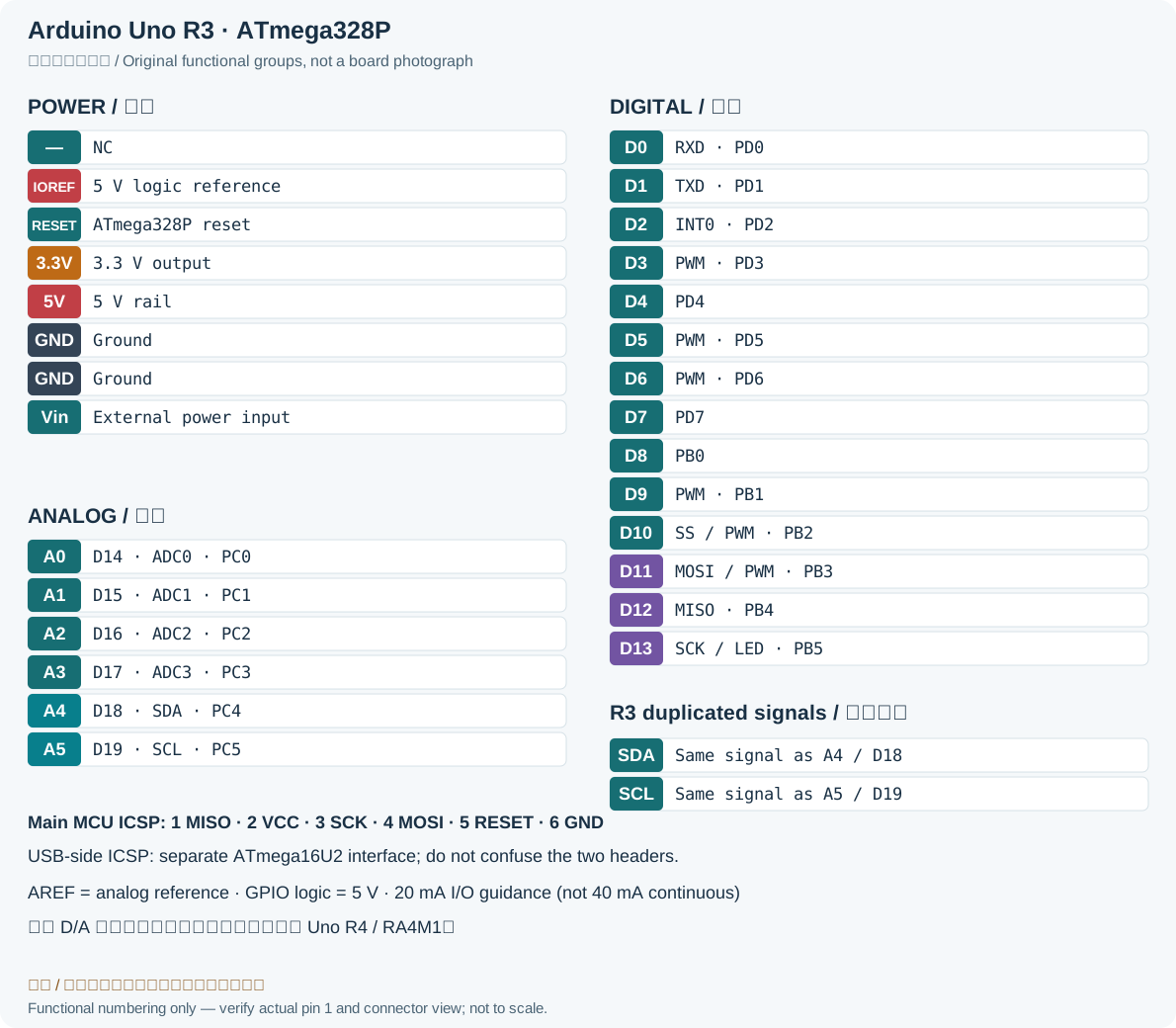
| Name | Function |
|---|---|
| - | Not connected |
| IOREF | Logic Reference (5V) (*) |
| RESET | PCINT14/RESET pin |
| 3.3V | 3.3V |
| 5V | 5V |
| GND | Ground |
| GND | |
| Vin | Input voltage (External power) |
| Name | MCU pin | Function |
|---|---|---|
| 14 (A0) | PC0 (23) | ADC0/PCINT8 |
| 15 (A1) | PC1 (24) | ADC1/PCINT9 |
| 16 (A2) | PC2 (25) | ADC2/PCINT10 |
| 17 (A3) | PC3 (26) | ADC3/PCINT11 |
| 18 (A4) | PC4 (27) | ADC4/SDA/PCINT12 |
| 19 (A5) | PC5 (28) | ADC5/SCL/PCINT13 |
| Name | MCU pin | Function |
|---|---|---|
| 0 | PD0 (2) | PCINT16/RXD |
| 1 | PD1 (3) | PCINT17/TXD |
| 2 | PD2 (4) | PCINT18/INT0 |
| 3 | PD3 (5) | PCINT19/OC2B/INT1 (PWM) |
| 4 | PD4 (6) | PCINT20/XCK/T0 |
| 5 | PD5 (11) | PCINT21/OC0B/T1 (PWM) |
| 6 | PD6 (12) | PCINT22/OC0A/AIN0 (PWM) |
| 7 | PD7 (13) | PCINT23/AIN1 |
| 8 | PB0 (14) | PCINT0/CLKO/ICP1 |
| 9 | PB1 (15) | OC1A/PCINT1 (PWM) |
| 10 | PB2 (16) | SS/OC1B/PCINT2 (PWM) |
| 11 | PB3 (17) | MOSI/OC2A/PCINT3 (PWM) |
| 12 | PB4 (18) | MISO/PCINT4 |
| 13 | PB5 (19) | SCK/PCINT5 (LED) |
| GND | Ground | |
| AREF | AREF (21) | Analog Ref. |
| 18 (A4) | PC4 (27) | ADC4/SDA/PCINT12 (*) |
| 19 (A5) | PC5 (28) | ADC5/SCL/PCINT13 (*) |
| Name | MCU pin | Function |
|---|---|---|
| 1 | PB4 (18) | MISO/PCINT4 |
| 2 | VCC (5 V) | |
| 3 | PB5 (19) | SCK/PCINT5 |
| 4 | PB3 (17) | MOSI/OC2A/PCINT3 |
| 5 | PC6 (1) | RESET/PCINT14 |
| 6 | Ground | |
| Name | Function |
|---|---|
| 1 | MISO2 |
| 2 | VCC (5 V) |
| 3 | SCK2 |
| 4 | MOSI2 |
| 5 | RESET |
| 6 | Ground |
Legacy source notes and applicability
These notes retain the legacy record. For corrected facts and applicability, use this page’s quick answer, scope and visible table corrections.
Arduino Uno (R3) Front View
Processor: ATmega328 (8-bit, 16MHz, 2KB RAM, 32KB Flash)
Features: 14 digital I/O pins, 6 analog input pins
POWER header:
ANALOG header:
DIGITAL header:
ICSP header:
ICSP header (USB interface):
Notes:
(*) pins available only on Rev.3
OCxA/OCxB can be used for PWM output.
Absolute max current per pin is 40 mA (20 mA recommended).
Absolute max current for the entire package is 200 mA.
Frequently asked questions
Can A0–A5 be digital pins?
On classic Uno R3 they can be digital pins 14–19. A4/A5 also share I²C SDA/SCL, so coordinate their configured function with connected peripherals.
How do the two ICSP headers differ?
The main ICSP connects to ATmega328P; the USB-side ICSP connects to ATmega16U2. Similar signal names lead to different chips, firmware and reset targets.
Does a PWM mark mean an analog voltage output?
No. OCxA/OCxB identifies timer-driven digital PWM. Load, filtering and the external circuit determine any average voltage; this is not a dedicated DAC.
Related tools and references
Sources and verification
- Arduino: Uno R3 / ATmega328P
- Arduino official Uno R3 pinout and current notes
- Arduino: I/O and power details
- Arduino: Uno R3 versus R4
Legacy baseline: the Electrodoc Pro 5.2 data package. Raw records are retained and checked factual corrections are shown explicitly.