PCB TOOLS / PINOUT & INTERFACE REFERENCE
SD Card Pinout: SD, miniSD, microSD and SPI
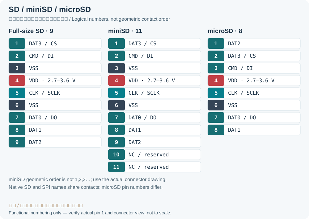
Check physical contacts and SD/SPI signals separately for each form factor: full-size SD has 9 contacts, miniSD 11 and microSD 8. Their contact numbers are not interchangeable.
Quick answer
microSD contacts 1–8 are DAT2, CD/DAT3, CMD, VDD, CLK, VSS, DAT0 and DAT1. If the card supports SPI, CS is contact 2, DI/MOSI is 3 and DO/MISO is 7. CS on contact 1 in the historical combined table applies to SD/miniSD only.
Scope
Use the separate form-factor tables below for physical numbering. The historical 11-row table is an SD/miniSD signal reference: full-size SD uses only 1–9, while 10/11 are miniSD NC contacts. It is not a microSD physical map. Additional UHS-II/SD Express contacts are outside this classic single-row reference.
Reading example
For a microSD card documented to support SPI, card 2 is CS, 3 connects to host MOSI, 5 is SCLK, 7 connects to host MISO, 4 is the specified VDD and 6 is GND. Do not copy full-size SD contact 1 CS and contact 2 DI numbering.
Checked reference tables
| Physical contact | SD-mode signal | SPI-mode signal (if supported) | Function |
|---|---|---|---|
| 1 | CD/DAT3 | CS | Data bit 3/detection function; active-low SPI select |
| 2 | CMD | DI / MOSI | SD command/response; SPI card input (host MOSI) |
| 3 | VSS | VSS | Supply ground |
| 4 | VDD | VDD | Specified card supply |
| 5 | CLK | SCLK | Clock |
| 6 | VSS | VSS | Supply ground |
| 7 | DAT0 | DO / MISO | Data bit 0; SPI card output (host MISO) |
| 8 | DAT1 | RSV | Data bit 1; reserved/unused in SPI |
| 9 | DAT2 | RSV | Data bit 2; reserved/unused in SPI |
| Physical contact | SD-mode signal | SPI-mode signal (if supported) | Function |
|---|---|---|---|
| 1 | CD/DAT3 | CS | Data bit 3/detection function; active-low SPI select |
| 2 | CMD | DI / MOSI | SD command/response; SPI card input (host MOSI) |
| 3 | VSS | VSS | Supply ground |
| 4 | VDD | VDD | Specified card supply |
| 5 | CLK | SCLK | Clock |
| 6 | VSS | VSS | Supply ground |
| 7 | DAT0 | DO / MISO | Data bit 0; SPI card output (host MISO) |
| 8 | DAT1 | RSV | Data bit 1; reserved/unused in SPI |
| 9 | DAT2 | RSV | Data bit 2; reserved/unused in SPI |
| 10 | NC | NC | Not connected; leave open |
| 11 | NC | NC | Not connected; leave open |
| Physical contact | SD-mode signal | SPI-mode signal (if supported) | Function |
|---|---|---|---|
| 1 | DAT2 | RSV | Data bit 2; reserved/unused in SPI |
| 2 | CD/DAT3 | CS | Data bit 3/detection function; active-low SPI select |
| 3 | CMD | DI / MOSI | SD command/response; SPI card input (host MOSI) |
| 4 | VDD | VDD | Specified card supply |
| 5 | CLK | SCLK | Clock |
| 6 | VSS | VSS | Supply ground |
| 7 | DAT0 | DO / MISO | Data bit 0; SPI card output (host MISO) |
| 8 | DAT1 | RSV | Data bit 1; reserved/unused in SPI |
Interfaces, pinouts and technical reference
SD mode
| Pin | Signal | Description |
|---|---|---|
| 1 | CD/DAT3 | Card detection / Data Line 3 |
| 2 | CMD | Command Line |
| 3 | VSS | Ground |
| 4 | VDD | 3.3V Supply (2.7-3.6v) |
| 5 | CLK | Clock |
| 6 | VSS | Ground |
| 7 | DAT0 | Data Line 0 |
| 8 | DAT1 | Data Line 1 |
| 9 | DAT2 | Data Line 2 |
| 10 | n.c. | miniSD only: NC; no such contact on full-size SD/microSDLegacy record: “Reserved”. The combined 11-row table cannot represent all three form factors. Contacts 10/11 are miniSD NC; use the separate physical pin tables. |
| 11 | n.c. | miniSD only: NC; no such contact on full-size SD/microSDLegacy record: “Reserved”. The combined 11-row table cannot represent all three form factors. Contacts 10/11 are miniSD NC; use the separate physical pin tables. |
SPI mode
| Pin | Signal | Description |
|---|---|---|
| 1 | CSLegacy record: “CD”. The SPI chip-select signal is CS. The source’s CD can be confused with card detection: physical contact 1 on SD/miniSD, but 2 on microSD. | Chip Select |
| 2 | DI | Data Input |
| 3 | VSS | Ground |
| 4 | VDD | 3.3V Supply (2.7-3.6v) |
| 5 | SCLK | Clock |
| 6 | VSS | Ground |
| 7 | DO | Data Output |
| 8 | - | Unused or IRQ |
| 9 | - | Unused |
| 10 | n.c. | miniSD only: NC; no such contact on full-size SD/microSDLegacy record: “Reserved”. The combined 11-row table cannot represent all three form factors. Contacts 10/11 are miniSD NC; use the separate physical pin tables. |
| 11 | n.c. | miniSD only: NC; no such contact on full-size SD/microSDLegacy record: “Reserved”. The combined 11-row table cannot represent all three form factors. Contacts 10/11 are miniSD NC; use the separate physical pin tables. |
Legacy source notes and applicability
These notes retain the legacy record. For corrected facts and applicability, use this page’s quick answer, scope and visible table corrections.
SPI mode
SPI mode is optional on microSD card
Frequently asked questions
Are miniSD contacts simply 1–11 from left to right?
No. Do not infer physical order by sorting contact numbers. The Hirose DM2 terminal drawing shows 9,1,2,3,10,11,4,5,6,7,8. Match the card contact view to the socket manufacturer’s drawing.
How do DI/DO correspond to MCU MOSI/MISO?
DI/DO are named from the card’s perspective: DI receives host data and corresponds to host MOSI; DO transmits card data to host MISO. DI is contact 2 on full-size SD/miniSD and contact 3 on microSD.
Related tools and references
Sources and verification
- SD Association: simplified specification and interface-mode reference
- Transcend: TS2GSDC manufacturer datasheet, contact table (distributor hosted)
- Hirose: DM2 miniSD manufacturer catalog, pages 3–4 (DigiKey hosted)
- Transcend: USD410M manufacturer datasheet, microSD contacts (distributor hosted)
Legacy baseline: the Electrodoc Pro 5.2 data package. Raw records are retained and checked factual corrections are shown explicitly.