PCB TOOLS / Electronics reference
Conventional PCI bus A/B contacts
Look up conventional PCI sides A/B, the 32-bit base and 64-bit extension, power, multiplexed AD and controls.
Quick answer
The base ends at 62 positions and 64-bit extension at 94; A/B labels do not establish card orientation from screen left/right.
Scope
For historical conventional PCI/optional 66MHz context, with voltage keying/version constraints; not a complete PCIe, miniPCI or PCI-X specification.
Reading example
At B44 read C/BE[1]#; the source signal incorrectly says[2], while its description already identifies byte enable1.
Legacy tables with visible corrections
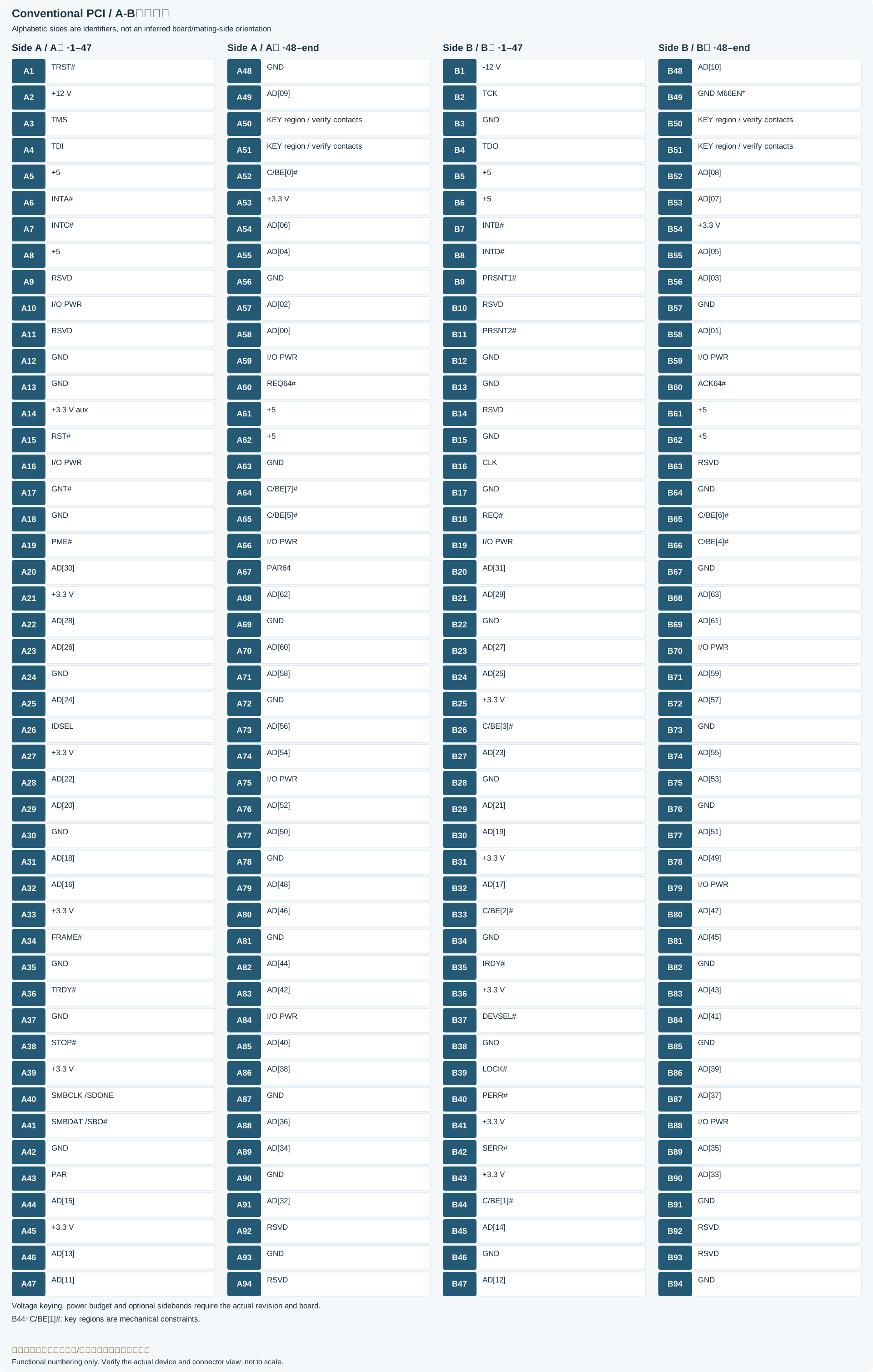
| Side B | Pin | Side A | ||
|---|---|---|---|---|
| Description | Name | Name | Description | |
| -12 volt power | -12 V | 1 | TRST# | Test Reset (JTAG1) |
| Test Clock (JTAG2) | TCK | 2 | +12 V | +12 volt power |
| Ground | GND | 3 | TMS | Test Mode Select (JTAG5) |
| Test Data Output | TDO | 4 | TDI | Test Data Input (JTAG3) |
| + 5 volt power | +5 | 5 | +5 | + 5 volt power |
| +5 | 6 | INTA# | Interrupt A | |
| Interrupt B | INTB# | 7 | INTC# | Interrupt C |
| Interrupt D | INTD# | 8 | +5 | + 5 volt power |
| Pulled low to indicate 7.5 or 25 W power required | PRSNT1# | 9 | RSVD | Reserved |
| Reserved | RSVD | 10 | I/O PWR | +V I/O (+5 V or +3.3 V) |
| Pulled low to indicate 7.5 or 15 W power required | PRSNT2# | 11 | RSVD | Reserved |
| Ground | GND | 12 | GND | Ground |
| GND | 13 | GND | ||
| Reserved | RSVD | 14 | +3.3 V aux | +3.3 volt power aux |
| Ground | GND | 15 | RST# | Bus reset |
| 33/66 MHz clock | CLK | 16 | I/O PWR | +V I/O (+5 V or +3.3 V) |
| Ground | GND | 17 | GNT# | Bus grant from motherboard to card |
| Bus request from card to motherboard | REQ# | 18 | GND | Ground |
| +V I/O (+5 V or +3.3 V) | I/O PWR | 19 | PME# | Power management event (optional) 3.3 V |
| Address/Data bus 31 (upper half) | AD[31] | 20 | AD[30] | Address/Data bus 30 (upper half) |
| Address/Data bus 29 (upper half) | AD[29] | 21 | +3.3 V | +3.3 volt power |
| Ground | GND | 22 | AD[28] | Address/Data bus 28 (upper half) |
| Address/Data bus 27 (upper half) | AD[27] | 23 | AD[26] | Address/Data bus 26 (upper half) |
| Address/Data bus 25 (upper half) | AD[25] | 24 | GND | Ground |
| +3.3 volt power | +3.3 V | 25 | AD[24] | Address/Data bus 24 (upper half) |
| Command, Byte Enable 3 | C/BE[3]# | 26 | IDSEL | Initialization Device Select |
| Address/Data bus 23 (upper half) | AD[23] | 27 | +3.3 V | +3.3 volt power |
| Ground | GND | 28 | AD[22] | Address/Data bus 22 (upper half) |
| Address/Data bus 21 (upper half) | AD[21] | 29 | AD[20] | Address/Data bus 20 (upper half) |
| Address/Data bus 19 (upper half) | AD[19] | 30 | GND | Ground |
| +3.3 volt power | +3.3 V | 31 | AD[18] | Address/Data bus 18 (upper half) |
| Address/Data bus 17 (upper half) | AD[17] | 32 | AD[16] | Address/Data bus 16 (upper half) |
| Command, Byte Enable 2 | C/BE[2]# | 33 | +3.3 V | +3.3 volt power |
| Ground | GND | 34 | FRAME# | Bus transfer in progress |
| Initiator ready | IRDY# | 35 | GND | Ground |
| +3.3 volt power | +3.3 V | 36 | TRDY# | Target Ready |
| Device selected | DEVSEL# | 37 | GND | Ground |
| Ground | GND | 38 | STOP# | Target requests halt (Stop Transfer Cycle) |
| Locked transaction | LOCK# | 39 | +3.3 V | +3.3 volt power |
| Parity error | PERR# | 40 | SMBCLK /SDONE | SMBus clock or Snoop done (obsolete) |
| +3.3 volt power | +3.3 V | 41 | SMBDAT /SBO# | SMBus data or Snoop backoff (obsolete) |
| System Error | SERR# | 42 | GND | Ground |
| +3.3 volt power | +3.3 V | 43 | PAR | Parity |
| Command, Byte Enable 1 | C/BE[1]#Legacy record: “C/BE[2]#”. B44 describes byte enable1, and the Freescale contact table confirms C/BE1; the source signal incorrectly says2. | 44 | AD[15] | Address/Data bus 15 (lower half) |
| Address/Data bus 14 (lower half) | AD[14] | 45 | +3.3 V | +3.3 volt power |
| Ground | GND | 46 | AD[13] | Address/Data bus 13 (lower half) |
| Address/Data bus 12 (lower half) | AD[12] | 47 | AD[11] | Address/Data bus 11 (lower half) |
| Address/Data bus 10 (lower half) | AD[10] | 48 | GND | Ground |
| Ground | GND M66EN* | 49 | AD[09] | Address/Data bus 9 (lower half) |
| Key notch for 5 V-capable cards | GND | 50 | GND | Key notch for 5 V-capable cards |
| GND | 51 | GND | ||
| Address/Data bus 8 (lower half) | AD[08] | 52 | C/BE[0]# | Command, Byte Enable 0 |
| Address/Data bus 7 (lower half) | AD[07] | 53 | +3.3 V | +3.3 volt power |
| +3.3 volt power | +3.3 V | 54 | AD[06] | Address/Data bus 6 (lower half) |
| Address/Data bus 5 (lower half) | AD[05] | 55 | AD[04] | Address/Data bus 4 (lower half) |
| Address/Data bus 3 (lower half) | AD[03] | 56 | GND | Ground |
| Ground | GND | 57 | AD[02] | Address/Data bus 2 (lower half) |
| Address/Data bus 1 (lower half) | AD[01] | 58 | AD[00] | Address/Data bus 0 (lower half) |
| +V I/O (+5 V or +3.3 V) | I/O PWR | 59 | I/O PWR | +V I/O (+5 V or +3.3 V) |
| Acknowledge 64-bit; no connect for 32-bit devices | ACK64# | 60 | REQ64# | Request 64-bit; no connect for 32-bit devices |
| + 5 volt power | +5 | 61 | +5 | + 5 volt power |
| +5 | 62 | +5 | ||
| Reserved | RSVD | 63 | GND | Ground |
| Ground | GND | 64 | C/BE[7]# | Command, Byte Enable 7 |
| Command, Byte Enable 6 | C/BE[6]# | 65 | C/BE[5]# | Command, Byte Enable 5 |
| Command, Byte Enable 4 | C/BE[4]# | 66 | I/O PWR | +V I/O (+5 V or +3.3 V) |
| Ground | GND | 67 | PAR64 | Parity 64 bit |
| Address/Data bus 63 | AD[63] | 68 | AD[62] | Address/Data bus 62 |
| Address/Data bus 61 | AD[61] | 69 | GND | Ground |
| +V I/O (+5 V or +3.3 V) | I/O PWR | 70 | AD[60] | Address/Data bus 60 |
| Address/Data bus 59 | AD[59] | 71 | AD[58] | Address/Data bus 58 |
| Address/Data bus 57 | AD[57] | 72 | GND | Ground |
| Ground | GND | 73 | AD[56] | Address/Data bus 56 |
| Address/Data bus 55 | AD[55] | 74 | AD[54] | Address/Data bus 54 |
| Address/Data bus 53 | AD[53] | 75 | I/O PWR | +V I/O (+5 V or +3.3 V) |
| Ground | GND | 76 | AD[52] | Address/Data bus 52 |
| Address/Data bus 51 | AD[51] | 77 | AD[50] | Address/Data bus 50 |
| Address/Data bus 49 | AD[49] | 78 | GND | Ground |
| +V I/O (+5 V or +3.3 V) | I/O PWR | 79 | AD[48] | Address/Data bus 48 |
| Address/Data bus 47 | AD[47] | 80 | AD[46] | Address/Data bus 46 |
| Address/Data bus 45 | AD[45] | 81 | GND | Ground |
| Ground | GND | 82 | AD[44] | Address/Data bus 44 |
| Address/Data bus 43 | AD[43] | 83 | AD[42] | Address/Data bus 42 |
| Address/Data bus 41 | AD[41] | 84 | I/O PWR | +V I/O (+5 V or +3.3 V) |
| Ground | GND | 85 | AD[40] | Address/Data bus 40 |
| Address/Data bus 39 | AD[39] | 86 | AD[38] | Address/Data bus 38 |
| Address/Data bus 37 | AD[37] | 87 | GND | Ground |
| +V I/O (+5 V or +3.3 V) | I/O PWR | 88 | AD[36] | Address/Data bus 36 |
| Address/Data bus 35 | AD[35] | 89 | AD[34] | Address/Data bus 34 |
| Address/Data bus 33 | AD[33] | 90 | GND | Ground |
| Ground | GND | 91 | AD[32] | Address/Data bus 32 |
| Reserved | RSVD | 92 | RSVD | Reserved |
| RSVD | 93 | GND | Ground | |
| Ground | GND | 94 | RSVD | Reserved |
Frequently asked questions
Are PCI and PCIe interchangeable?
No.The parallel bus and serial link differ mechanically, electrically and in protocol.
Why does M66EN appear with GND?
It reflects legacy 33/66MHz implementation differences; interpret it per revision and board, not by forcing a level.
Related tools and references
Sources and verification
Legacy baseline: the Electrodoc Pro 5.2 data package. Raw records are retained and checked factual corrections are shown explicitly.